23.2Solid-State Electronics
Electronic Devices: Diodes — American System Physics Revision Notes & Topical Questions
10 min read 7 parts Lesson 4 of 5 1 quiz
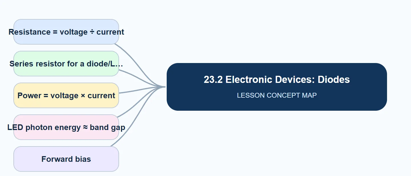
Describe how a depletion layer forms at a p-n junction.Resistance = voltage ÷ currentR = V/I (Ω); a diode's resistance is not constant (non-ohmic).Series resistor for a diode/LEDR = (Vsupply − Vdiode) / I.In a series circuit the supply p.d.
- Power = voltage × current
- LED photon energy ≈ band gap
- Forward bias
- Reverse bias
- Half-wave rectification
- Full-wave rectification
Part 1 of 7Key ideas
Part 2 of 7Learning objectives
Part 3 of 7Essential knowledge
- This leaves positive donor ions on the n-side and negative acceptor ions on the p-side,
- forming the depletion layer with an electric field that stops further diffusion.
- When forward biased, electrons crossing the junction recombine with holes and drop by an energy about equal to the band gap, emitting a photon.
- Different band gaps give different colours; blue LEDs need larger gaps than red.
- (and higher threshold p.d.)
Part 4 of 7Process & sequence
Formation of the depletion layerwrite these steps in this order; each step is a marking point.
Part 5 of 7Worked examples
- p.d. across resistor = 9.0 − 2.0 = 7.0 V. R = V/I = 7.0/0.020 = 350 Ω. P = VI = 7.0 × 0.020 = 0.14 W.What the symbols mean: P = power (W) · I = current (A) · V = potential difference (V)
- E = hc/λ = (6.63 × 10−34 × 3.00 × 108)/530 × 10−9 = 3.75 × 10⁻¹⁹ J. V = E/q = 3.75 × 10⁻¹⁹/1.60 × 10−19 = 2.3 V.What the symbols mean: E = photon energy (J) · h = 6.63 × 10⁻³⁴ J s · c = 3.00 × 10⁸ m s−1 · λ = wavelength (m)
- p.d. across diode ≈ 0.7 V, so p.d. across resistor = 5.0 − 0.7 = 4.3 V. I = 4.3/470 = 9.1 × 10⁻³ A (9.1 mA).
Part 6 of 7Summary
Part 7 of 7Compare: Compare
| Feature | Forward bias | Reverse bias |
|---|---|---|
| Connection | p to +, n to − | p to −, n to + |
| Depletion layer | Narrows (disappears above threshold) | Widens |
| Resistance | Low (above about 0.7 V) | Very high |
| Current | Large, rises steeply | Almost zero (tiny leakage) |
| Device | How used | Application |
|---|---|---|
| Silicon diode | Forward/reverse | Rectifiers, protection against wrong polarity |
| LED | Forward biased with series resistor | Indicators, displays, lighting, remote controls |
| Photodiode | Reverse biased | Light meters, optical fibre receivers, cameras |
| Solar cell | Unbiased, generates p.d. | Converts light energy to electrical energy |
Key terms
Command terms
Exam technique
Keywords the mark scheme looks for in this lesson
How to get full marks (examiner guidance)
Words to avoid
Instant feedbackCheck yourself
Q1. A silicon diode is forward biased when
Show answer
A. Forward bias: p to +, n to −.
Q2. What happens to the depletion layer in reverse bias?
Show answer
B. Carriers are pulled away from the junction.
Q3. The output of a half-wave rectifier is
- A. steady d.c.
- B. a.c. at double frequency
- C. pulses of current in one direction with gaps
- D. zero
Show answer
C. One diode conducts only in alternate half-cycles.
Q4. How many diodes are in a bridge rectifier?
- A. 1
- B. 2
- C. 3
- D. 4
Show answer
D. Four diodes, two conducting in each half-cycle.
Q5. An LED needs 2.0 V at 10 mA from a 6.0 V supply. The series resistor is
- A. 400 Ω
- B. 600 Ω
- C. 200 Ω
- D. 800 Ω
Show answer
A. R = (6.0 − 2.0)/0.010 = 400 Ω.
Q6. A photodiode's current increases in bright light because
Show answer
B. Absorbed photons generate carriers.
Marked practiceQuizzes for this lesson
Last updated: