Skip to content
Dabour HubLEARN · PRACTICE · EXPLORESign inStudent

23.3Solid-State Electronics

Transistors, Logic Gates and Integrated Circuits — American System Physics Revision Notes & Topical Questions
10 min read 7 parts Lesson 5 of 5 1 quiz

🩺
100% Curriculum Specification Match Lesson Doctor Verified
The only platform with 100% curriculum specification match and verified interactive question banks.
0%read
Lesson summary

Describe the structure of an npn transistor and use β = IC/IB.Current gain = collector current ÷ base currentβ = IC/IB (no unit).Emitter current = collector current + base current: IE = IC + IB (A).Potential divider outputVout = Vin × R2/(R1 + R2) (V), where R2 is the resistor th…

  • Base resistor
  • Logic gates
  • Bipolar junction transistor (BJT)
  • Base current (IB)
  • Current gain (β)
  • Transistor as a switch

Section 1 of 7Transistors, Logic Gates and Integrated Circuits

Essential knowledge
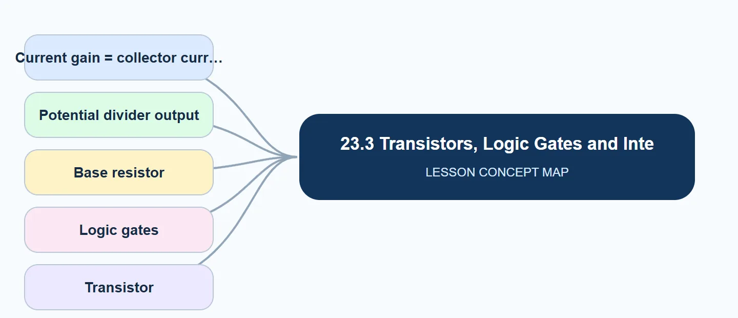
23.3 Transistors, Logic Gates and Integra… concept map: Current gain = collector curr, Potential divider output, Base resistor, Logic gates, Transistor
Visual guide to the key ideas explained in this lesson.
An npn transistor is a thin p-type base sandwiched between an n-type emitter and an n-type collector. The base–emitter junction behaves like a diode: it must be forward biased by about 0.7 V for the transistor to conduct.
When a small base current flows, electrons from the emitter flood into the very thin base; most do not recombine but are swept on into the collector. So a small base current controls a collector current typically 100 times larger.
As a switch, the transistor is either off (base below 0.7 V, no collector current) or fully on (saturated). This allows a weak signal from a sensor circuit to switch a high-current device like a motor, relay or lamp.
Sensor circuits use a potential divider containing a thermistor or LDR. The output p.d. changes as temperature or light changes, and when it crosses 0.7 V the transistor switches. Replacing the fixed resistor with a variable resistor lets you adjust the switching point.
A relay is often used on the collector side so that the small transistor current can switch a separate high-voltage circuit; a diode is placed across the relay coil to protect the transistor from the induced voltage when switching off.
As an amplifier, the transistor is biased partly on so that a small varying input produces a large, similar-shaped varying output. Microphones, radios and speakers rely on this.
Digital electronics represents information as 0s and 1s. Digital signals are less affected by noise than analogue signals because small distortions do not change a clear high or low; they can be regenerated exactly.
Logic gates
NOT inverts; AND gives 1 only if all inputs are 1; OR gives 1 if any input is 1; NAND is NOT-AND; NOR is NOT-OR. Gates can be combined; for example, an alarm that sounds when a door is open AND it is dark uses an AND gate.
To analyse a combined circuit, label intermediate points, build a truth table with columns for each point, and work through all input combinations systematically (00, 01, 10, 11).
Integrated circuits (ICs) are made by photolithography, printing billions of tiny transistors and connections onto a silicon wafer. They are small, cheap, reliable and fast, and form the processors and memory of computers and phones.

Section 2 of 7Process & sequence

1
Place an LDR and a fixed resistor in series across the supply to form a potential divider; connect their junction to the transistor base through a base resistor.
2
Connect a lamp or relay between the positive supply and the collector; connect the emitter to 0 V.
3
In bright light, the LDR resistance is low, so the p.d. across it is small; if the LDR is between base and 0 V, the base p.d. stays below 0.7 V.
4
With the base below 0.7 V, no base current flows and the transistor is off, so the lamp is off.
5
When it gets dark, the LDR resistance rises, so the p.d. across it rises above 0.7 V.
6
Base current flows, the transistor switches on, and a large collector current lights the lamp.
  • Swap the LDR and resistor to make a light-activated switch instead.

Transistor dark-activated switch sequencewrite these steps in this order; each step is a marking point.

1
Light level falls.
2
LDR resistance increases.
3
p.d. across the LDR (base p.d.) rises above 0.7 V.
4
Small base current flows; transistor switches on.
5
Large collector current flows, lighting the lamp.

Section 3 of 7Compare

Truth tables for logic gates (A, B inputs)
ABANDORNANDNOR
000011
010110
100110
111100

NOT gate

  • one input;
    • output is the opposite (0 → 1, 1 → 0).
  • NAND = AND followed by NOT;
    • NOR = OR followed by NOT.

Transistor uses
UseHow it operatesExample
SwitchBase p.d. above/below 0.7 V turns collector current on/offAutomatic night light with an LDR
AmplifierSmall changes in IB give large changes in ICMicrophone amplifier, hearing aid
LogicCombinations of transistors act as gatesComputer processors, memory

Section 4 of 7Worked examples

6.04 mA
A transistor has a current gain of 150. The base current is 40 µA. Calculate the collector and emitter currents.
  • IC = βIB = 150 × 40 × 10−6 = 6.0 × 10⁻³ A (6.0 mA). IE = IC + IB = 6.0 mA + 0.040 mA = 6.04 mA (6.0 × 10⁻³ A).
1.0 V
A potential divider has a 10 kΩ resistor (top) and a thermistor (bottom) across a 6.0 V supply. The output is taken across the thermistor. At 20 °C the thermistor is 2.0 kΩ. Find Vout and state whether the transistor is on.
  • Vout = 6.0 × 2.0/(10 + 2.0) = 6.0 × 0.167 = 1.0 V. This exceeds 0.7 V, so the transistor is on.
An alarm must sound (output 1) when switch A is on AND sensor B is NOT activated. Write the truth table.
  • Output = A AND (NOT B). Rows: A=0,B=0 → 0; A=0,B=1 → 0; A=1,B=0 → 1; A=1,B=1 → 0. Only one row gives 1.

Section 5 of 7Key terms

Section 6 of 7Command terms

Command terms
Identify / Describe (FRQ)
A short, specific statement; describing requires relevant characteristics, not a single word.
Explain / Justify (FRQ)
Give the cause-and-effect reasoning or evidence; a restated fact does not score.
Calculate
Show setup, substitution and the answer with units.
Predict
State the expected outcome; add a reason only if asked to justify.
MCQ technique
Read every option; eliminate distractors that are true statements but do not answer the question; watch for NOT/EXCEPT.

Section 7 of 7Exam technique

Keywords the mark scheme looks for in this lesson

Keywords the mark scheme looks for in this lesson
Transistor · Bipolar junction transistor (BJT) · Base current (IB) · Current gain (β) · Amplifier · Transistor as a switch · Logic gate · Truth table · Digital signal · Analogue signal · Integrated circuit (microchip) · Potential divider
Learn each definition in the Key words tab exactly; a missing keyword in a definition usually loses the mark.

How to get full marks (examiner guidance)

1
Answer exactly what is asked; extra correct material does not earn credit, and contradictory statements can cancel credit (AP FRQ).
2
Use precise vocabulary, never “it/stuff/things”.
3
Show units and working in calculations.
4
In MCQs, predict the answer before reading the options, then eliminate.

Words to avoid

1
the transistor makes energy to amplifythe transistor uses energy from the power supply; the small input only controls the larger current.
2
the base current is largea small base current controls a much larger collector current.
3
OR gate gives 1 only if one input is 1OR gives 1 if at least one input is 1 (including both).
4
LDR resistance increases in bright lightLDR resistance decreases as light intensity increases.
5
IE = IC − IBIE = IC + IB.

Last updated: